Sensitivities: Lumpiness of earnings
The key sensitivities as we see them are lumpiness of earnings, market cycles, dependence on key suppliers and customers and foreign exchange exposure. The first two are the most significant. Since a single production MBE system can cost €2.2–3.5m, depending on configuration (an R&D system is typically <€1m), and 90% of revenue is recognised on delivery, turnover can fluctuate substantially from quarter to quarter and the final outcome each year is very dependent on Riber meeting its delivery schedule for individual units. Demand for evaporators is linked to the OLED and solar equipment cycles. Demand for MBE equipment is less dependent on individual cycles because it is deployed in more markets, each following different phasing.
Company description: Global number one in MBE
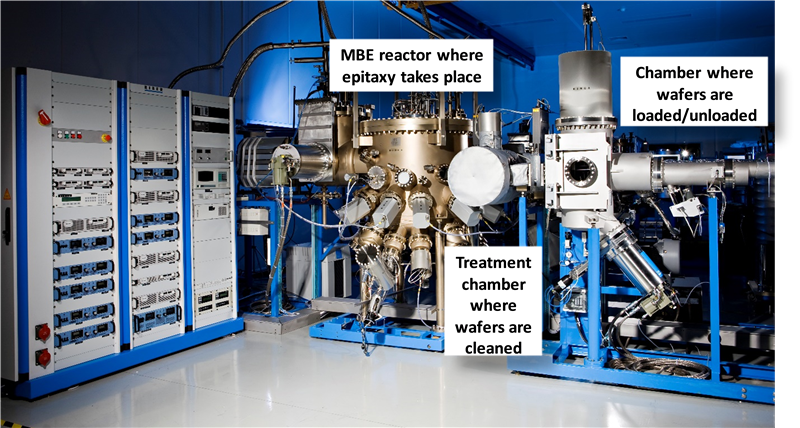
Riber develops and manufactures MBE machines and evaporators, both of which are used in the manufacture of semiconductors. It is the global market leader for MBE equipment, with the largest installed base of MBE machines in operation (c 750) and more than 50% market share. The MBE portfolio ranges from competitively priced research reactors to substantially larger production machines. Over 80% of the installed MBE base is deployed in universities, research institutes and the research labs of major global corporations. The remainder is deployed in the production facilities of electronic component manufacturers and providers of epitaxial wafers. MBE equipment is used to create compound semiconductor material for a wide range of applications including high-frequency 4G and 5G communications chips, terrestrial and submarine fibre-optic networks, light detection and ranging (LiDAR) and night vision sensors. Riber’s dominant share in the global MBE market is attributable to it having the broadest range of MBE systems, which enables the deposition of the widest range of types of alloys. The evaporators are incorporated in equipment for processing thin-film solar cells, OLED displays for smartphones and tablets and OLED lighting. They are sold either to the equipment integrator or direct to the end-user. Riber also derives revenues from providing services to its large installed base of clients.
Exhibit 1: Company timeline
Date |
Milestone |
1964 |
Formation of company making ultra-high vacuum equipment. |
1976 |
Development of first commercial MBE deposition systems. |
1978 |
Launch of world’s first turnkey MBE system. |
1990s |
Launch of world’s first high-throughput MBE production reactor. |
2000 |
Listed on NYSE-Euronext Paris. |
2004 |
Acquisition of Addon to extend product portfolio and gain access to OLED market. |
2008 |
Acquisition of VG Semicon from Oxford Instruments to expand service activity. |
2009 |
Launch of first thin-film evaporator systems. |
2015 |
Acquisition of assets of MBE Control Systems to strengthen service activity in the US. |
February 2019 |
Acquisition of assets of SemiPro to strengthen service activity in the US. |
Date |
1964 |
1976 |
1978 |
1990s |
2000 |
2004 |
2008 |
2009 |
2015 |
February 2019 |
Milestone |
Formation of company making ultra-high vacuum equipment. |
Development of first commercial MBE deposition systems. |
Launch of world’s first turnkey MBE system. |
Launch of world’s first high-throughput MBE production reactor. |
Listed on NYSE-Euronext Paris. |
Acquisition of Addon to extend product portfolio and gain access to OLED market. |
Acquisition of VG Semicon from Oxford Instruments to expand service activity. |
Launch of first thin-film evaporator systems. |
Acquisition of assets of MBE Control Systems to strengthen service activity in the US. |
Acquisition of assets of SemiPro to strengthen service activity in the US. |
Source: Edison Investment Research
Riber’s headquarters are in Bezons in the suburbs of Paris, where it owns a 3,500m2 facility, including a 1,000m2 clean room with the capacity to output 25 MBE machines annually. The company designs and assembles equipment in Bezons, outsourcing the manufacture of individual non-key components. It has subsidiaries in China (opened H218), Korea and the US, and a network of around 30 agents and distributors. More than 90% of revenues are generated from exports to customers elsewhere in Europe and in the US, Canada, Mexico, Japan, China and South Korea. It currently employs around 120 people.
MBE key tool for creating multi-layer structures
Semiconductor devices consist of very thin films of compound semiconductor materials with differing electronic and optical properties stacked up like a many-layered cake. The behaviour of a device is determined by how electrons move through each layer. For example, a transistor acts as a switch by only allowing electrons to pass through a stack when a voltage is applied across the top and bottom layers of the stack. Different structures where electrons are converted to light energy as they pass through specific layers form light-emitting diodes (LEDs) and lasers. Varying the composition of the layer where electricity to light conversion takes place causes a different colour of light, including ultra-violet (UV) or infra-red (IR) wavelengths, to be produced. These complex structures cannot be realised using standard silicon chip fabrication technology. Specialist equipment such as MBE or metal organic chemical vapor deposition (MOCVD – for a comparison with MBE see below) reactors are required.
|
|

|
Source: Edison Investment Research
|
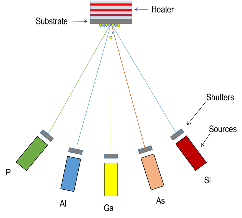
Device performance depends on achieving very precise control over the thickness and composition of each layer. MBE achieves this by generating individual streams of molecules by heating solid or gaseous materials, directing these beams onto a substrate material and turning the stream on and off with a computer-controlled shutter or valve with a very quick response time (typically 0.6 seconds). For example, a layer of gallium arsenide is created by directing beams of gallium (Ga) and arsenic (As) onto the substrate. When the atoms arrive on the substrate, they combine to form gallium arsenide (GaAs). Small amounts of other elements may be added to the mixture. For example, adding aluminium (Al) results in the formation of a layer of gallium aluminium arsenide (GaAlAs), which is commonly used in GaAs-based red and IR laser diodes. The entire process takes place in an ultra-high vacuum to ensure very high levels of purity of the individual layers.
MBE market: Size and growth
Since Riber’s MBE equipment may be used to manufacture a wide range of compound semiconductor materials, it is deployed in many markets that have different profiles. This reduces the company’s exposure to any single market but makes it more difficult to predict overall demand beyond the period covered by the order book. Typical applications are 5G/4G/Wi-Fi communications, satellite transceivers, FTTH (fibre-to-the-home), LAN (local area network) and submarine fibre-optic networks, laser cutting, infrared and UV detectors used in night vision systems, thermography, medical diagnosis, vegetation mapping, LiDAR systems and magnetic sensors. One of the markets where Riber is well placed to benefit from customers expanding R&D and production capacity is optical fibre networks. According to a report from Future Market Insights published in February 2020, the global FFTH market is expected grow at a CAGR of 15% between 2019 and 2029 from a base of over US$12bn in 2018. Factors driving growth include rising demand for higher bandwidth and the increased use of fibre for cloud computing services. Riber’s MBE equipment is used to deposit the vital layers that convert electricity to light in optical components.
Emerging markets for MBE equipment include the use of GaN material for UV applications and micro-LEDs. The application areas for UV LED systems have increased steadily over the past five years. The dominant application is UV curing, which includes printing, adhesives and coatings. Other applications are disinfection and purification, which are driven by the rising need to stop water- and air-borne diseases. Market growth has benefited from the worldwide ban on mercury vapour lamps after 2020, combined with reduced prices of UV LEDs and their increased adaptability, efficiency and longevity, which have been made possible by the adoption of next-generation substrates. A report from BIS Research published in February 2018 predicted that the global UV LED market will reach $1,163.5m by 2023. A report by Technavio published in November 2018 predicted that the global UV LED technology market will show a CAGR of 37% between 2017 and 2022. This report cited new applications such as treating seeds, improving the shelf life of agricultural produce and spectroscopy. Clearly any global recession resulting from the pandemic may cause growth to be slower in the initial period covered by any projections, but we believe that the overall direction of travel will be the same.
With regard to the micro-LED market, which is in its infancy, a report from Research and Markets published in February 2020 predicts that this will grow by US$18.7bn between 2019 and 2025, a CAGR of 78.8%. The key market driver here is the development of display technology that can deliver brighter pictures with less power consumption. In the nearer term, near-to-eye cameras and virtual reality and mixed reality (a fusion of actual and virtual worlds) headsets for professional applications are likely to be the dominant applications, but in the longer term, incorporation of micro-LEDs in consumer devices such as laptops, smartphones and home theatres will become commonplace if, as assumed in the report, the price point reduces to a level where this is economically viable.
Recent independent data on the projected growth rate of the MBE market is scarce. Management notes that demand for R&D equipment is generally stable with total global sales of 10–15 units each year. Purchases are driven by new projects instigated in response to technological challenges: for example, a requirement to shift to larger diameter substrates or renewal of equipment originally purchased in the 1980s or 1990s. There is also demand from economies such as China and India, which are seeking to develop their own compound semiconductor capability. Demand for production equipment is similar to the semiconductor cycle, though linked to various types of compound semiconductor devices discussed below, so is more variable. Management notes that the global requirement is typically three to six systems each year.
Exhibit 3: Riber MBE equipment
|

|
|
|
MBE market: Competitive position
There are relatively few other companies globally manufacturing MBE equipment. According to a Yole Développement study published in 2012, US-listed Veeco is the only other company offering high-capacity/high-throughput MBE production tools for manufacturing. Management estimates that in FY19 Riber had 86% share of this segment. Management believes that this dominant position is attributable to the production output, yield and cost of ownership afforded by the equipment as well as the services and maintenance provided.
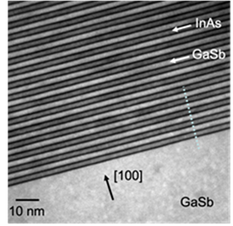
Exhibit 4: InAsGaSb epitaxial structure created using MBE
|
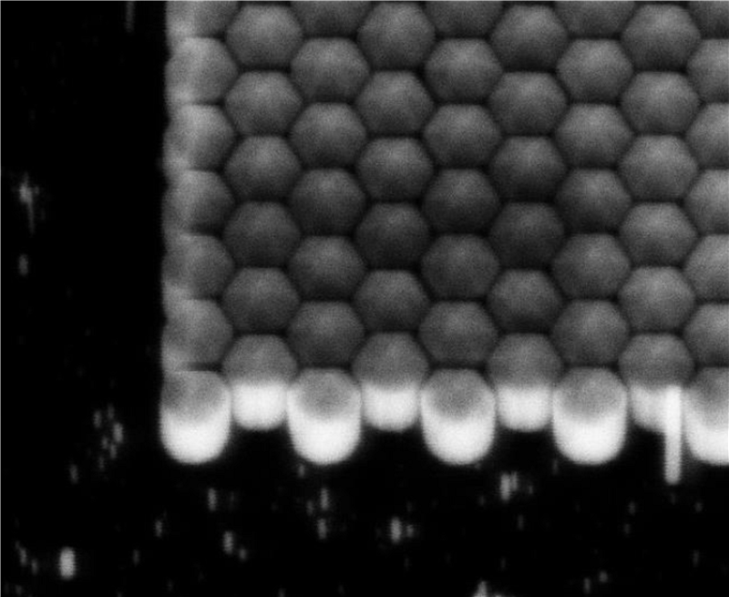
Exhibit 5: Nanowires created using MBE
|

|

|
|
|
|
Exhibit 4: InAsGaSb epitaxial structure created using MBE
|

|
|
|
Exhibit 5: Nanowires created using MBE
|

|
|
|
There are around 10 other manufacturers offering R&D or pilot-production systems. These include DCA Instruments (Finland), Dr. Eberl MBE-Komponenten (Germany), Eiko (Japan), Scienta Omicron (Germany), SVT Associates (US) and Veeco. Riber has the dominant share of this segment (79% in FY19 according to management estimates) as well. Management believes that the company commands the dominant position in this segment because it supports production of the widest range of alloys including III-V and II-VI compound semiconductors, gallium nitrides, mercury/cadmium/telluride (MCT), SiGe and oxide alloys. As in the production segment, the technical barriers to entry are extremely high, deterring new market entrants. Moreover, given the relatively small size of the market globally, we believe it is unlikely that an equipment manufacturer would regard the return as economically worthwhile.
Competitive epitaxial technologies
The main alternative to MBE for creating epitaxial layers is MOCVD. In this technique gases are injected into a chamber containing the substrate, which is heated. When the mixture of gases meets the surface of the hot substrate it reacts, depositing a thin layer of the desired alloy on the substrate. For example, a mixture of trimethylindium (In(CH3)3) and phosphine (PH3) reacts to form indium phosphide (InP) and methane (CH4). The indium phosphide is deposited on the substrate and the methane gas is removed from the reactor. We note the following key differences between the two techniques:
■
Throughput: MOCVD can deposit material more quickly than MBE, so for structures such as LEDs, which are composed of relatively thick layers of materials, it is the preferred technology.
■
Uniformity: the MBE technique results in the deposition of a much more uniform layer across the surface of a single wafer or multiple wafers being processed simultaneously. This in turn gives superior yield.
■
Precision: as the MBE technique enables a reactor to switch between source materials more cleanly than MOCVD it is more suitable for devices with thin and alternating layers eg PHEMTs. Additionally, since MBE takes place at a lower temperature than MOCVD, there is less mixing between layers at an interface, giving more precise control of the final structure. This is attractive for higher performance device structures such as 850nm vertical cavity surface emitting lasers (VCSELs) for data communications and 940nm VCSELs for high power applications.
■
Material range: MBE enables a wider range of elements to be deposited since the stream of molecules is created by simply heating a sample of the material (eg indium or phosphorus) that is to be deposited. In the MOCVD technique the active elements (indium and phosphorus) need to be converted into a gas containing other elements (hydrogen and carbon). This is not always possible. For example, it is very difficult to get stable antimonide gases. Antimonide-based infra-red detectors are key materials for aerospace sensors and systems, remote sensing, thermal imaging, infrared spectroscopy and LiDAR.
■
Cost: MBE reactors are larger and more expensive than MOCVD reactors because the former operate in an ultra-low vacuum. However, this is partly offset by the more rigorous safety measures required for MOCVD because of the toxic and flammable nature of the gases used.
We note that a high proportion of Riber’s MBE reactors are sold for R&D purposes, reflecting the wider range of materials that may be deposited using this technique and the higher levels of control over the deposition process. Within the production environment, the higher throughput of MOCVD reactors has obvious attractions, but MOCVD is not suitable for all types of epitaxy. We note that reactors being installed for the first phase of IQE’s Newport facility are for volume VCSEL production and use MOCVD technology for VCSEL (opto-electronic) epitaxy, while MBE reactors are deployed at some of IQE’s other locations where they are used for a variety of applications including IQE’s new and emerging technologies. One of these emerging applications, cREO, uses a combination of MBE and MOCVD capabilities.
Diversification into evaporators
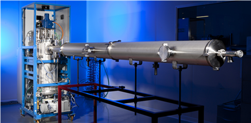
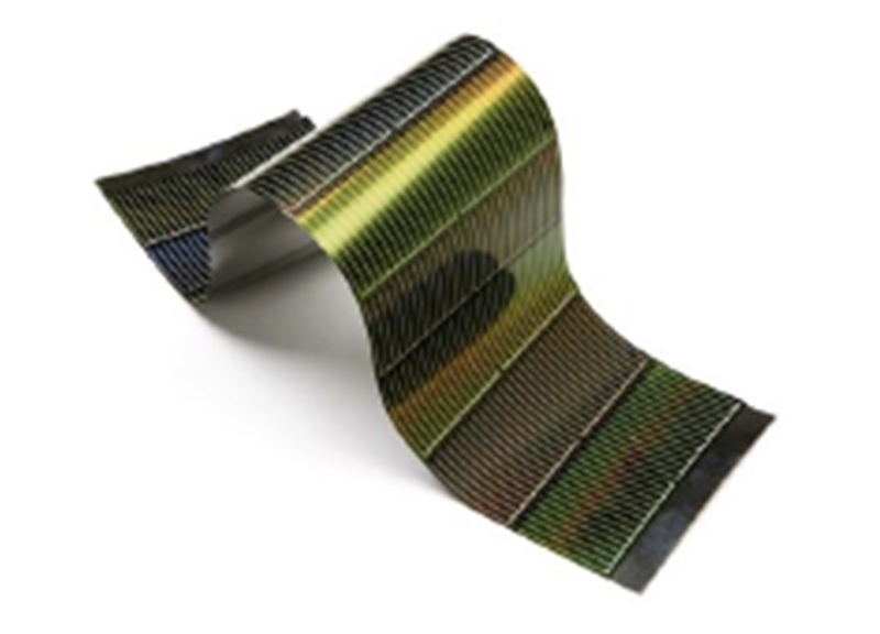
Riber has adapted the effusion cells used to generate streams of material inside MBE systems so that they can be used to deposit highly uniform, ultra-thin films of material on much larger substrates. Arrays of point source evaporators are used to deposit the aluminium forming electrical contracts in OLED displays and lights. Riber sells evaporators to systems integrator Canon Tokki, which serves OLED manufacturers in South Korea and China. It also sells linear evaporators for copper indium gallium selenide (CIGS) thin-film solar cell processes to systems integrator Singulus Technologies, primarily for deployment in China.
Evaporator market
Management estimates that the market size is several thousand point source evaporators per year depending on investment cycles in the OLED and solar industries and the emergence of new applications. The market is dominated by two larger Asian-based competitors. Since Riber’s principal customer stopped ordering evaporators in H218 because of weakness in its own order book, Riber’s current market share is minimal. Riber expects sales to pick up towards the end of 2020. Management believes that Riber’s point source evaporators deposit films that are more uniform with respect to thickness and exhibit a lower number of defects than films deposited by competitive equipment and that Riber is the only manufacturer to have developed a high precision linear evaporator for depositing the selenium used in CIGS type solar cells.
MBE: R&D
Management’s objective in this segment is to maintain Riber’s global market share above c 60%. This is partly to secure further R&D sales and partly to ensure it stays close to the projects that progress to production so it is well placed to sell production equipment with the appropriate enhancements. The company’s strategy for taking market share is to invest in innovation, typically making relatively small adjustments to components and accessories to support novel processes. For example, it is adapting R&D equipment so it has the same level of automated process control as production models. As part of this programme it is working with LAAS-CNRS in Toulouse on enhancements to its proprietary control software that will monitor layer growth in real-time and feedback the data to control production temperatures and thus layer growth. Once finalised, this capability would be added to production equipment as well, providing a significant competitive advantage.
MBE: Production
Riber is focusing its sales resource on mainland Europe, where there is a lot of activity in the opto-electronics market, and in China, where the government is developing its own semiconductor industry so it is not dependent on products from companies such as Qorvo or Skyworks. The potential impact of a no-deal Brexit is therefore very limited. Riber is less active in the US where there is a lot of spare MBE capacity, for example at one of IQE’s sites, although it has acquired service operations in the territory to support existing customers. (See Exhibit 6 for an analysis of the customer base.)
|
Clients |
Operational units |
Sample customers |
MBE for R&D |
324 |
630 |
Chinese Academy of Sciences, Fraunhofer Institute, Ioffe Physico-Technical Institute, Russian Academy of Sciences, The University of Tokyo, US Naval Research Laboratory |
MBE for production |
44 |
120 |
III-V lab, Acken Optoelectronics, Asahi Kasei, Aselsan, Coherent, IntelliEPI, IQE, Northrop Grumman, Phillips Photonics, QDLaser, Raytheon, Teledyne Technologies, Trumpf |
Evaporators |
9 |
c 2,000 |
Canon Tokki, First Solar, Heliatek, Singulus Technologies |
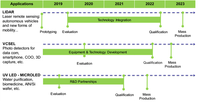
Riber is attempting to catalyse market growth higher than the historical average by working with partners to develop new MBE applications. We note that it typically takes seven to 10 years for an initial idea to pass into volume production. Three of the areas closest to commercialisation are LiDAR, VCSELs and UV LEDs. Exhibit 7 shows the expected timescale for meeting major milestones on each of these programmes.
LiDAR
During H119, Riber commenced on-site testing of an MBE49 variant for the Belgian research institute IMEC for work on antimonide alloys that will potentially be deployed in LiDAR for autonomous vehicles. The project involves work on the stack of layers forming the laser to improve the response time and optimising the process so 4” substrates can be used instead of 2” ones, thus improving throughput. This potentially brings down the cost of production to a price point suitable for widespread adoption. A report from Grand View Research published in March 2020 notes that the global LiDAR market was valued at US$1.1bn in 2019 and is expected to register a CAGR of 13.2% between 2020 and 2027. The main driver for this growth is navigation and positioning systems in autonomous vehicles.
Opto-electronics: VCSELs
In our January Outlook note on IQE we observed the widespread adoption of VCSELs had been triggered by a switch to 6” substrates, which increased MOCVD throughput, thus supporting a price-point appropriate for mass adoption. However, as noted earlier, uniformity issues with MOCVD have a deleterious impact on yield. Riber is working with IntelliEPI on a new MBE system able to process eight 6” VCSEL wafers simultaneously. This will substantially improve throughput, potentially making MBE a more cost-effective process for manufacturing VCSELs. In December 2019 MarketsandMarkets predicted the global VCSEL market would rise at a CAGR of 16.9% from $1.8bn in 2018 to $3.9bn by 2023. Growth was attributed mainly to the rising adoption of arrays of VCSELs in proximity sensing and medical applications, data communications, infrared illumination in automobiles for pedestrian detection, collision avoidance, parking assistance, traffic sign recognition and lane departure warning.
Exhibit 7: Timescale for commercialising new industrial markets
|

|
|
|
UV LEDs and micro-LEDs
As noted earlier, most LEDs are manufactured using MOCVD technology. However, it is easier to achieve high levels of doping with MBE technology than MOCVD. Riber is working with the Centre de Recherches sur l’HétéroEpitaxie et ses Applications (CRHEA), part of the Université Côte d’Azur on the fabrication of red and green coloured micro-LEDs with the highly doped active layers processed using MBE, the others using MOCVD. CRHEA has installed MBE equipment from Riber that is capable of handling the 8” wafers commonly used in MOCVD processes to give high throughput. The project with CRHEA also involves the development of UV LEDs as these require high levels of doping to create structures that emit the correct wavelength (colour) light. CRHEA is creating a demonstration UV LED wafer for evaluation by a potential commercial customer interested in using UV light to purify water.
Evaporators
Exhibit 8: Linear evaporator
|
Exhibit 9: Flexible substrate with evaporated layers for CIGS PV (photo-voltaic)
|

|

|
|
|
|
Exhibit 8: Linear evaporator
|

|
|
|
Exhibit 9: Flexible substrate with evaporated layers for CIGS PV (photo-voltaic)
|

|
|
|
The strategic focus for this product line is the development of a next-generation linear evaporator that extends the potential market. Riber is working on a medium-temperature linear evaporator to extend the range of applications of this technology to other industrial sectors. Target markets include battery manufacturing and silicon wafer production where the technology has the potential to deliver more homogenous substrate doping.
Services and accessories
Management has identified this activity as giving potential for delivering high-margin revenue that is less dependent on the overall level of investment in compound semi-conductor, OLED display or sola cell-manufacturing equipment. Its stated objective is to grow annualised revenues by 35% over the next three years, thus providing a substantial proportion of annual fixed costs. The company has created a dedicated sales and marketing team to actively promote the offer across the company’s extensive installed base. This includes training, consultancy, retro-fit sales of hardware and software, on-site upgrades, in-factory component repairs and refurbishments and preventative or remedial operations at client sites. The acquisition of US-based SemiPro in February 2019 is supportive of this goal, as well as furthering the drive to sell MBE equipment in the region.
CEO Philippe Ley: A graduate of Ecole Nationale Supérieure d’Arts et Métiers, one of the Grandes Écoles, Philippe Ley started his career at the international engineering company ASSYSTEM in 1994. He moved to Renault Automation in 1997, where he occupied different managerial positions and became head of engineering at COMAU France, an industrial automation company, in 2001. He joined Riber in 2007 where he was first production director, then operation director and member of the executive board. He left Riber in 2015 to become managing director at ERCA, which produces equipment for manufacturing containers for dairy food. He returned to Riber in 2018 as chief executive officer and member of the executive board, taking over as president in June 2019.
Chairman Michel Picault: A graduate of Institut National des Sciences Appliquées Lyon, one of the Grandes Écoles, Michel Picault’s first employment was a research post with a government organisation, followed by an R&D role with a French telecom company. Between 1983 and 1997 he worked for Riber in a range of capacities including technical, after-sales service, sales and marketing and production in both the US and France. In 1997 he led a buy-out of Riber and was appointed president of the company. He stepped down from this position in 2008, while remaining member of the executive board until 2014. He left Riber in 2014, working as an adviser for small companies and on funding for start-ups. In 2016 he was invited to re-join the executive board, to help turn the company round, and was reappointed president of the executive board in 2018. While stepping down from this position in June 2019, he remains a member of the executive board. He is scheduled to retire at the end of December 2020. A replacement has not been appointed yet.


